FPGA/SoC + DDR PCB Design Tips - Phil's Lab #59
Video Not Working? Fix It Now
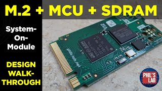
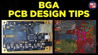
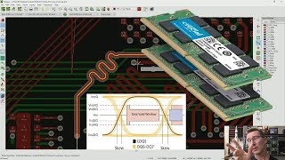
FPGA/SoC with DDR3 memory PCB design overview, basics, and tips for a Xilinx Zynq-based System-on-Module (SoM).
Mixed-signal hardware design course: https://phils-lab-shop.fedevel.education
[SUPPORT]
Free trial of Altium Designer: https://www.altium.com/yt/philslab
Patreon: https://www.patreon.com/phils94
[LINKS]
Advanced PCB design course survey: https://forms.gle/3Kdq1E9KV9TAhiim9
Rick Hartley video: https://www.youtube.com/watch?v=ySuUZEjARPY
Previous FPGA/SoC video: https://youtu.be/Wt6aske1K10
GitHub: https://github.com/pms67
[TIMESTAMPS]
00:00 Introduction
00:30 Altium Designer Free Trial
00:50 Advanced PCB Design Course Survey
01:30 System Overview
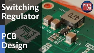
02:37 Power Supplies (Schematic)
03:50 Power Supplies (PCB)
06:33 Vias as Test Points
07:04 Layer Stack-Up
08:55 Impedance Calculation and Via Types
10:22 GND Layers and Power Distribution
13:30 BGA and Decoupling Layout
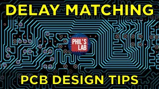
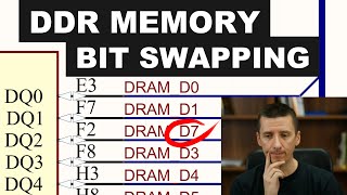
16:12 Routing, Colours, Packag Delays, and Time Matching
22:00 DDR Termination
23:11 0.5mm Pad Pitch Tip
24:18 Final Tips
ID: QIBvbJtYjWuHiTG0uCoK
Comment