KiCad 9: Design & assemble an ESP32 IoT 4-layer PCB loaded with goodies **A Complete Guide**
Video Not Working? Fix It Now
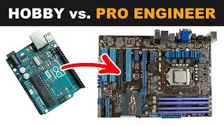
In this comprehensive video, Peter from Tech Explorations takes you through the entire process of designing a custom IoT PCB using KiCad 9. From schematic creation to PCB layout, routing, and preparing for manufacturing, this video covers it all. Whether you're a beginner or an experienced PCB designer, you'll find valuable insights and practical tips to enhance your workflow.
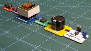
This project features a four-layer IoT development board powered by the ESP32-C3-S2, complete with sensors, power management, and user interface components. Peter also shares his experience with KiCad 9 Release Candidate, highlighting its new features and improvements.
Stay tuned for a follow-up video where Peter will showcase the manufactured PCB and perform testing.
For the full write-up of this project, visit the blog post at https://txplo.re/kicad9-project
If you found this video helpful, please like, share, and subscribe to the channel for more content like this!
---
Chapters:
00:00:00 - Introduction
00:00:08 - Overview of the IoT PCB Design
00:03:57 - Component Placement and Design Challenges
00:06:02 - Design Guidelines and Workflow Overview
00:07:01 - Operational Requirements and Component Selection
00:17:49 - Researching and Sourcing Components
00:30:40 - Setting Up KiCad 9 for the Project
00:38:05 - Creating the Schematic
01:10:54 - Designing the ESP32 Circuitry
01:49:35 - Adding Sensors and User Interface Components
02:15:15 - Validating the Schematic and Assigning Footprints
02:30:22 - Setting Up the PCB Layout Editor
03:05:57 - Component Placement and Board Outline Refinement
03:40:44 - Routing and Copper Zones
04:00:37 - Differential Pairs and High-Speed Signal Routing
04:11:26 - Power Traces and Signal Routing
05:05:07 - Design Rule Check and Final Refinements
05:08:13 - Design for Manufacturing (DFM) Checks
05:20:18 - Adding Silkscreen and Final Touches
05:36:54 - 3D Model Configuration and Visualization
05:50:00 - Preparing Files for Manufacturing
05:51:56 - Conclusion and Next Steps
---
Resources Mentioned:
1. NextPCB Website: https://www.nextpcb.com
2. NextPCB PCB Capabilities Page: https://www.nextpcb.com/pcb-capabilities
3. NextPCB HQ DFM Tool Download: https://www.nextpcb.com/dfm-tool
4. Espressif ESP32 Documentation: https://www.espressif.com/en/support/documents/technical-documents
5. Espressif ESP32 Module Placement Guidelines: https://www.espressif.com/en/support/explore/documentation/module-placement
6. Texas Instruments High-Speed Layout Guidelines: https://www.ti.com/lit/an/szza009/szza009.pdf
7. SnapEDA (Component Search and Libraries): https://www.snapeda.com
8. KiCad Official Website: https://www.kicad.org
9. Tech Explorations Blog on NextPCB DFM Tool: https://techexplorations.com/blog/nextpcb-dfm-tool
10. Espressif ESP32 Boot Mode Documentation: https://t-explore/esp32boot
---
For the full write-up of this project, visit the blog post at https://txplo.re/kicad9-project
If you enjoyed this video, please like, share, and subscribe to the channel for more tutorials and projects!
Comment